
The World's Most Important Machine
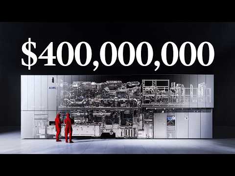
This is a video about the most complicated commercial product humanity's ever built.
26 capitulos
- Understanding Microchips and Moore's LawTransistor FoundationMicrochips contain billions of transistors that function as ones and zeros in computers. Electrons whiz between transistors, and smaller transistors allow faster computation and increased density per chip.Moore's Law PrincipleFor over 50 years, transistors became smaller and the number that could fit on a chip doubled every two years. This pattern, identified by Intel co-founder Gordon Moore in 1965, became a primary driver of the tech industry.The Breakthrough ProblemAround 2015, progress stopped, and Moore's Law hit a brick wall. A single company's revolutionary machines saved the industry by enabling continued miniaturization.Machine Specifications• Costs $400 million • Hits 50,000 tin droplets per second • 150,000 laser shots per second with zero misses • Mirrors are the smoothest objects in the universe • Overlay accuracy of five atoms or less
- Microchip Manufacturing ProcessRaw Material PreparationSilicon dioxide from sand is purified into nearly 100% silicon chunks, then melted in a special furnace. A seed crystal is lowered into the vat where silicon atoms attach and extend the crystal structure as it's slowly raised and rotated.Wafer Processing Steps• Ingot is cut into wafers using diamond wire saws, producing up to 5,000 wafers • Each wafer is carefully polished • Coated with photoresist material • Exposed to light through a patterned mask to weaken specific areas • Rinsed with basic solution to remove exposed photoresistLayer Creation CycleThe main steps repeat for each layer: coat, expose, etch, and deposit. The process occurs 10 to 100 times depending on the chip, with transistors requiring the most complicated bottom layer.Critical StepPhotolithography, where light shines through the mask onto the wafer, is the hardest and most crucial step. It determines how small features can be made on the chip.
- Photolithography and Diffraction PhysicsLight Behavior ChallengeAs features become smaller, the gaps in the mask approach the wavelength of light, causing problems. Light wavefronts bend as they pass through gaps, creating diffraction patterns where peaks and troughs can cancel out (dark spots) or reinforce (bright spots).Wavelength Advantage• Shorter wavelengths allow printing of smaller patterns • Red laser has 650 nanometer wavelength • Green laser has 532 nanometer wavelength • Shorter wavelengths produce closer-spaced diffraction orders • Industry settled on 193 nanometer deep UV light by late 1990sPhysics PrinciplesDiffraction is inevitable, so designers use it strategically by working backwards from desired patterns. The Rayleigh Equation determines the smallest feature size achievable. Numerical aperture (NA) determines how much light can be captured to print smaller features.Fundamental LimitThere is a hard limit when numerical aperture reaches one and the lens would need to be infinite. To continue shrinking features, shorter wavelengths are the only option.
- The X-Ray Lithography VisionKinoshita's IdeaIn the 1980s, Japanese scientist Hiroo Kinoshita proposed using much shorter wavelengths like x-rays around 10 nanometers to print much smaller features. This theoretical approach faced major obstacles.Fundamental Obstacles• X-rays at these wavelengths have enough energy to eject electrons, causing absorption in most materials • Air absorbs these wavelengths, requiring vacuum conditions • Lenses cannot focus these x-rays because they would absorb them • The idea seemed impossible to implementMirror SolutionAround 1983, Kinoshita discovered that curved mirrors can focus x-rays like lenses do. Jim Underwood and Troy Barbee's work on special mirrors that could reflect x-rays of 4.48 nanometers provided the breakthrough approach.Constructive InterferenceBy creating alternating layers of tungsten and carbon at specific thicknesses, x-rays reflected from different boundaries could constructively interfere. Underwood and Barbee used 76 alternating layers to reflect approximately 6% of x-rays, proving the concept.
- Kinoshita's Early Success and SkepticismFirst AchievementKinoshita designed and built three tungsten-carbon curved multi-layer mirrors to reflect 11 nanometer light. With these mirrors, he managed to print lines 4,000 nanometers thick, proving x-ray lithography was theoretically possible.Audience RejectionIn 1986, Kinoshita presented his findings to the Japanese Society of Applied Physics. The audience was highly skeptical and refused to believe his results, with people regarding the whole thing as a 'big fish story.'Scientific Barriers• This light isn't naturally produced by anything on Earth • Scientists had to build an artificial sun using particle accelerators or synchrotrons • Each machine would need its own power source • Incredibly smooth mirrors were needed to focus and print tiny featuresMirror Smoothness RequirementsFor Kinoshita's mirrors to minimize scattering, they needed to be atomically smooth with average bumps of only 2.3 silicon atoms thick. For comparison, normal household mirrors have average heights of about 4,000 silicon atoms.
- Lawrence Livermore and Bell Labs PartnershipLivermore's MissionLawrence Livermore National Lab, founded by Ernest Lawrence and Edward Teller, was built for nuclear weapons research. Scientists there studied x-ray light released during nuclear fusion reactions but had never been able to capture and analyze it.Hawryluk's WorkAndrew Hawryluk and his team used multilayer mirrors to reflect some x-ray light within a few years. In 1987, a visiting Cornell professor challenged him, asking 'Can you do anything useful with this stuff?' which inspired Hawryluk to write a white paper applying the mirrors to lithography.Initial RejectionWhen Hawryluk presented his findings at a conference, the response was extremely negative. Every person he looked up to came to the microphone and told him why it wouldn't work and called it a stupid idea. This was the low point of his career.Bell Labs OpportunityThree days after the failed presentation, Bill Brinkman from Bell Labs, who was the Executive Vice President of AT&T, called Hawryluk and invited him to New Jersey to give a talk. At Bell Labs, Hawryluk found fellow believers in the technology.
- Government Support and Early Industry PartnershipCold War InvestmentThe US government had invested billions into national labs over 30 years to maintain technological edge during the Cold War. By the late 1980s, the Cold War was slowing down and these labs had research with commercial potential.Private-Public PartnershipThe government encouraged labs to partner with US companies to turn research into products and stimulate the economy. Bell Labs partnered with Hawryluk's lab and two others to develop x-ray lithography, with the government providing seed money.Technology RenamedBy 1993, the first international conference for x-ray lithography was held in Japan near Mount Fuji. Kinoshita said technology would advance from micro to nano to pico. The technology was given a new name: extreme ultraviolet lithography or EUV.Funding CrisisIn 1996, the US government cut funding for the project, spelling disaster for big chip companies like Intel. The industry estimated 193 nanometer lithography tools would fall behind Moore's Law by 2005 with no alternatives available.
- Industry Investment and the Engineering Test StandPrivate Sector RescueIntel, Motorola, AMD and other companies invested $250 million to keep EUV development going. This was the largest investment ever by private industry in a Department of Energy research project.First Prototype AchievementBy 2000, labs produced the Engineering Test Stand, the first fully functioning EUV prototype. It produced 9.8 watts of 13.4 nanometer EUV light reflected by eight mirrors from source to mask to wafer, proving EUV could work.Critical FlawThe prototype could only print about 10 wafers per hour. To be economically viable, it would need to print hundreds of wafers per hour, 24/7, 365 days a year, making the machine far from commercial readiness.Light Loss Problem• Each mirror had reflectivity of around 70%, which is close to maximum • After nine bounces, only 4% of light reached the wafer • Out of every 100 photons, only four made it to the wafer • Light loss made the prototype impractical for manufacturing
- ASML and the Wavelength ChoiceCompany EmergenceASML, originally standing for Advanced Semiconductor Materials Lithography, was located in the Netherlands. It spun off from Philips in the 1980s with little more than a shed and a barely working wafer stepper, but Philips gave them talented people like Jos Benschop and Martin van den Brink.Strategic PartnershipASML joined the US EUV consortium and became tasked with commercializing EUV. They partnered with German company Zeiss, where Zeiss would handle mirrors and ASML would focus on the light source.Wavelength Decision• Early days explored wavelengths between 5 and 14 nanometers • Four nanometer wavelength had only 20% maximum reflectivity • Silicon and molybdenum had 70% theoretical maximum for 13 nanometers • Molybdenum and beryllium had 80% for 11 nanometers but beryllium is extremely toxic • Scientists focused on silicon and molybdenum for 13 nanometer wavelengthMirror ManufacturingZeiss used sputtering process where plasma or ions bombard a target, ejecting atoms that stick to the mirror. The process is messy, creating bumps and gaps, but Dutch engineers perfected ion beam technique to shake atoms into proper positions.
- Light Source Generation MethodsThree Generation Methods• Synchrotron: quickly ruled out because each machine needs its own source • Discharge-produced plasma: heated metal vapor with electric field, but difficult to scale beyond a few watts • Laser-produced plasma: high powered laser hitting target material, only method that seemed scalableLaser-Produced Plasma DetailsA high-powered laser hits a target material, creating plasma hotter than 220,000 degrees Celsius. Electrons have so much energy that the nucleus cannot hold them, and up to 14 electrons escape their orbits before recombining to produce light.Xenon Limitations• Engineering Test Stand used 1,700 watt laser fired into xenon gas • Conversion efficiency was terrible at only 0.5% • Xenon emits mostly at 11 nanometers instead of needed 13-14 nanometer range • Neutral xenon atoms reabsorb the 13.4 nanometer light producedTin AdvantageTin has much higher emission peak around 13.5 nanometers, resulting in 5-10 times higher conversion efficiency than xenon. Like xenon, neutral tin atoms absorb EUV light, so ASML proposed shooting one tiny tin droplet at a time instead.
- Tin Droplet Formation and ChallengesDroplet Creation MethodExtremely pure tin is melted and pushed through a microscopic nozzle by high pressure nitrogen. The nozzle vibrates at high frequency to break the stream into tiny droplets, but the process is chaotic producing irregular droplets.Self-Organization MagicIrregular droplets coming out of the nozzle somehow self-organize into perfectly spaced, regular droplets of the same size and shape traveling at the same velocity before reaching the laser hit point. This self-organization is controlled by nozzle pressure and vibration frequency.Droplet Speed RequirementsDroplets must travel extremely fast because if the next droplet coming down the line is too close, it gets disturbed and messes up the next plasma event. The requirement is both making 50,000 droplets per second and having them travel at very high speed.Mirror Contamination Problem• Where does the tin go after hitting the droplet? • 30 centimeters away sits an atomically flat, very expensive mirror • Early days saw mirrors coated with tin very quickly • Need to keep collector mirrors almost perfectly clean for a year of operation • Liters of tin pass through the plasma event
- Hydrogen Gas Cleaning SystemCleaning MechanismLow pressure hydrogen gas is used to slow and cool tin particles down. Even if something makes it to the collector, the hydrogen pulls it off to form a gas called stannane, allowing the machine to clean collectors while running.Balancing Act• Too little hydrogen allows mirrors to get too dirty • Too much hydrogen absorbs too much EUV light • Excess hydrogen causes the system to overheat • Pressure and flow rate must be precisely controlledShockwave DiscoveryEngineers using an ultra-fast camera discovered that after every plasma event, a shockwave propagates through the hydrogen gas and is extremely repeatable. The Taylor-von Neumann-Sedov formula used to explain point source explosions in nuclear blasts matched the data perfectly.Hydrogen Flow RequirementsThe hydrogen must be flushed at incredibly high speeds around 360 kilometers per hour, more than a Category 5 hurricane, though at low density. This extreme flow is necessary to manage the energy from 50,000 tiny supernovas per second happening in the vessel.
- Achieving 100 Watts and Mirror PrecisionPower MilestoneBy 2013, ASML reached 50 watts by shooting 50,000 tin droplets per second. However, progress stalled with industry improvements in multi-patterning with 193 nanometer wavelength making EUV only useful if the source reached at least 200 watts and achieved 125 wafers per hour.Heat and Alignment IssuesIncreased power meant more heat, which shifted the mirrors slightly resulting in misaligned light and misaligned chip layers. Moving goalpost made it difficult because the industry found other solutions and wouldn't wait for EUV development.Zeiss Nervous SystemZeiss built a nervous system directly into the optics using robot-guided sensors that constantly measure the exact position and angle of each mirror down to the nanometer at the pico-radian, which is extremely precise.Extreme Accuracy ExampleA thought experiment shows the precision required: place a laser on the side of a mirror, aim it to the Moon, put a dime there, and the laser can decide whether to point to one side of the dime or the other side, requiring pico-radian pointing accuracy.
- The Pancake Solution and Double Down DecisionTin Density ProblemThe tin droplets were too dense, meaning most of the emitted EUV light was reabsorbed by neutral atoms before reaching the collector mirror. The way they blasted the droplet produced not enough light and too much debris.Breakthrough InnovationInstead of hitting the droplet once, hit it twice. The first shot flattens the droplet into a pancake shape, then the second more powerful main pulse evaporates the pancake to turn it into plasma.Pancake Advantage• Larger surface area for laser to vaporize • No added cost of more debris or neutral atoms • Tin is vaporized all at once • By 2014, reached coveted 100 watts markNext Generation BetASML decided to double down and invest in the next generation high NA EUV machine before even getting the current one to work. A crazy person was working on the next generation where they could not even make the EUV light in the first place.
- Customer Investment and Divine InterventionFunding CrisisASML reached out to customers saying they want this technology for next generation chips, so they must invest more. Intel invested around 4.1 billion dollars, and Samsung and TSMC invested another 1.3 billion combined.Customer PatienceWith no product to show, customers were running out of patience. Engineers were crucified at every conference when they could not live up to promises from the previous year, showing the same results repeatedly.Chapel CandlesAround 2012 or 2013, Kinoshita visited ASML while they struggled with EUV power. During dinner near a Maria Chapel, Kinoshita lit three candles for the three suppliers pursuing EUV technology at the time to invoke divine intervention.Correlation and Moving Targets• Strong correlation between lighting the candle and power going up • 200 watts milestone reached by 2014 • Industry improvements meant EUV needed at least 200 watts and 125 wafers per hour • Moving goalpost meant industry found other solutions and wouldn't wait
- Droplet Targeting and Precision TimingLaser Curtain TrackingDroplets travel through a maelstrom of hydrogen flow at tremendously high speeds. ASML uses laser curtains to track droplets, where scattered photons tell engineers when and where the droplet is located.Precision RequirementThe analogy is landing a golf ball in a hole 200 meters away, not just landing on the green but landing in the hole every time. The precision required is like shooting golf balls through a tornado and hitting the hole exactly when it arrives.Timing Calculation• Must account for how long light pulse takes to hit droplet after sending pulse • Laser curtains show when droplet passes through • Scattered photons tell engineers when to fire the laser • Droplets traveling extremely fast in hydrogen maelstrom2015 MilestoneBy 2015, they were getting closer to the 200 watt mark when ASML board members were summoned to Korea. Customers were really thin on patience, saying they either show 200 watts now or they go away. The experiment was still running when they left, and they had results demonstrating 200 watts when they landed.
- Oxygen Cleaning and Commercial ViabilityCollector Mirror DegradationHigh energy photons and hydrogen ions zipping around deteriorated the special top coating on the collector mirror. Mirrors had to be cleaned every 10 hours, which was terrible for productivity.Lucky DiscoveryAn engineer noticed that every time they opened up the machine, the mirrors suddenly seemed cleaner. He realized that whenever they opened the machine, oxygen comes in and the problem is solved.Oxygen Solution• Asked Martin van den Brink if they could add just a little oxygen to the system • Experimented with amount of oxygen needed in the vacuum • Found the right amount to keep collector clean much longer • Machine could run continuously for extended periodsCommercialization AchievementWith the oxygen fix, ASML's machine could run continuously much longer and finally became commercially viable. By 2016, orders started pouring in and all advanced chips now need ASML's machine, making them perhaps the most important tech company in the world.
- Low NA and High NA EUV MachinesFirst Commercial MachinesASML's first commercial machines had a numerical aperture of 0.33 and could print 13 nanometer lines. These are called the low NA machines and ASML still manufactures them for customers.High NA DevelopmentThe high NA machine with numerical aperture of 0.55 was the next generation, starting development in 2012. This larger optic system allows printing even smaller features for next generation chips.Price and Specifications• High NA machine costs over 350 million euros • Costs can be purchased directly by customers • High NA machine can print 8 nanometer features • First high NA machine was built and demonstratedMachine ImprovementOne improvement from ASML's first EUV machine to the newest is the number of pulses hitting the droplet. First pre-pulse flattens droplet into pancake, second pre-pulse reduces density further, and final pulse ionizes all of it for more EUV light.
- Clean Room ManufacturingCleanliness StandardsASML's machines are built in a super strict clean room. In any cubic meter, there can be no more than 10 particles only 0.1 microns large, and nothing bigger than that.Comparison Context• Pollen spec is around 20 microns • Extremely fine sand is around 10 microns • Hospital operating rooms allow maximum 10,000 particles per cubic meter at 0.1 microns • ASML clean room is vastly more stringentClean Room ProtocolAccess is strictly limited with only a few people allowed to go inside. Visitors must go through air showers where super clean air blows to brush down remaining particles on skin and clothing.Assembly ProcessMachines are assembled, tested and approved in the clean room. After approval, they are disassembled to ship around the world via 250 containers spread over 25 trucks and seven Boeing 747s.
- System Architecture and Light PathLaser SystemA carbon dioxide laser of just a few watts enters an amplifier where it bounces around until roughly five times its original power. It goes through four different amplifiers to bring the final laser up to 20,000 watts, four times stronger than lasers that cut through steel.Light Source ModuleThe laser pulses travel to the light source module where tin droplets are hit. The setup requires all of this enormous infrastructure just to make EUV light at the needed wavelength and power.Optics Path• Light bounces off collector mirror • Moves to illuminator with mirrors that shape and focus light • Light hits reticle carrying the chip design • Light enters projection optics box with mirrors that shrink the patternFinal DeliveryHigh NA machine shrinks pattern eight times in vertical direction and four times in horizontal direction. Light finally hits the wafer where the reticle whips back and forth at accelerations of over 20 Gs to print around 185 wafers per hour.
- Mirror Quality and Overlay PrecisionMirror Smoothness Comparison• Low NA mirrors the size of Germany would have largest bump about a millimeter high • High NA mirrors the size of the world would have largest bump about the thickness of a playing card • Improvement comes from decades of research and precision manufacturingNumerical Aperture IncreaseBy combining mirror improvements with mirror system architecture, ASML increased numerical aperture from 0.33 in low NA to 0.55 in high NA machines. This allows printing smaller features with the same wavelength.Overlay RequirementThe most any two chip layers can be offset, called the overlay, is one nanometer. That is five silicon atoms of precision, which is absolutely insane for layers hundreds of nanometers apart.Precision Budget• System engineers divide total one nanometer budget among different subsystems • Each subsystem gets fraction of total nanometer allowance • Engineers must fight for their part of the nanometer • Total accuracy across all systems must meet five atom precision
- Droplet Pulse Optimization and ScalingThree-Pulse SystemFirst pre-pulse flattens the droplet into a pancake, second pre-pulse further reduces the density turning it into low density gas, and final pulse ionizes all of it. For basically the same power from drive laser, they get even more EUV light.Current Capabilities• Most recent EUV light sources around 500 watt level • Increased rep rate up to 60,000 times per second • Roadmap plans to go to 100,000 droplets per second • Already demonstrated 100,000 droplets per second in labFuture ScalingTo get even more light, the only way is to hit more droplets. That is exactly what they did, increasing from 50,000 to 60,000 droplets per second, with 100,000 droplets per second coming next.Engineering ChallengeIncreasing droplet rate while maintaining timing precision and plasma quality is an enormous engineering challenge. The system must track and hit each droplet with laser pulses at exact moments.
- System Size and Component ComplexityMachine DimensionsThe full EUV lithography machine is huge and fills an entire clean room. The humongous beauty has taken many decades of development and many billions of dollars to build.Component Count• 5,000 companies supply 100,000 parts • 3,000 cables integrated throughout • 40,000 bolts holding everything together • Two kilometers of hosing for fluids and gasesInverse RelationshipSmaller you want to go, the larger everything around it becomes. This inverse proportionality means to print eight nanometer features requires massive infrastructure and precise control systems.Transportation ChallengeMachines are disassembled to ship around the world. High NA machine ships in 250 containers spread over 25 trucks and seven Boeing 747s, requiring complex logistics and reassembly at customer sites.
- First Customer Installation and Long JourneyInstallation TimelineASML decided on EUV around 2001, facing many challenges during development. In 2010, they installed the first system at a customer in Korea, thirteen years into the pursuit.Initial Success MomentWhen the first EUV machine was installed at a customer fab producing wafers, Jos realized they had made the right bet. This moment proved the decades of development was worthwhile.Hidden ChallengesThe person who helped install the first machine later revealed that after the team left after Christmas, the machine broke down and took two months to get back up again. They almost fired him for making the wrong decision.Path to Products• First system installed at customer in 2010 • Still had hurdles to resolve • First phone with EUV chips came out in 2019 • Nine years between first customer installation and consumer products
- The Power of Unreasonable ThinkingImpossibility to RealityAfter months of work on this video, it still feels absolutely impossible. The reasonable thing is to think none of it is possible and to point out all the problems with each aspect of the technology.Unreasonable PeopleThe reasonable man adapts himself to the world. The unreasonable one persists in trying to adapt the world to himself. Therefore, all progress depends on the unreasonable man.Historical Impact• If Andy and Kinoshita and all the others had been reasonable, we would have none of this technology • Imagine if everyone on Earth was reasonable, it would probably be extremely boring • Most technology and enjoyable things today wouldn't exist • We owe our lives to unreasonable people who refused to accept limitationsPersonal LessonMost technology we have nowadays would seem completely unreasonable even just 200 years ago. It is a reminder that it is good to be a little unreasonable, at least in the big parts of life.
- Learning Through Challenges and Brilliant SponsorshipBreakthrough ProcessChanging the world is difficult and took overcoming thousands of obstacles and over 30 years to get EUV to work. Big breakthroughs usually start by learning, exploring related ideas, applying them in new ways, and building skills for bigger challenges.Knowledge Building• Bit by bit, you gain knowledge • Learn by exploring related concepts • Apply ideas in new ways • Build skills for increasingly bigger challengesBrilliant PlatformBrilliant helps you excel in math, science and computer science with visual, interactive learning personalized for you. It is a powerful way to reach learning goals, whether mastering math for class or contributing to next technological breakthroughs.Learning Method• Learn by doing, proven far more effective than passive learning • Starts at right level based on background • Designs practice sets and reviews customized for you • Helps advance at ideal pace • Always something new to discover