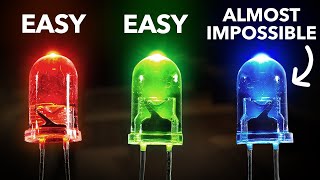
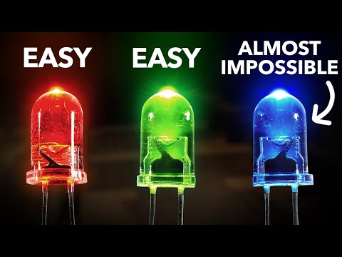
Why It Was Almost Impossible to Make the Blue LED
LEDs don't get their color from their plastic covers.
18 capitulos
- The LED Color ProblemHistorical Timeline• 1962: Nick Holonyak created the first visible red LED • Years later: Monsanto engineers created green LEDs • For decades: Only red and green colors were availableWhy Blue MatteredBlue LEDs would allow mixing red, green, and blue to create white light and every other color, unlocking LED use in light bulbs, phones, computers, TVs, and billboards.Industry Challenge• 1960s: IBM, GE, Bell Labs raced to create blue LED • Worth billions of dollars • After 30 years: Still no success despite thousands of researchersFailed ForecastMonsanto director claimed LEDs would never replace kitchen lights and would only be used in appliances, car dashboards, and stereo indicators.
- Understanding LED TechnologyLight vs HeatLight bulbs work by heating a tungsten filament until it glows, but most radiation is infrared heat. Only a negligible fraction is visible light, making them inefficient.How LEDs Work• LED = Light Emitting Diode • Diode has two electrodes allowing current to flow in one direction • When electrons fall from conduction band into holes, band gap energy is emitted as photonsEnergy BandsWhen atoms form a solid, valence and conduction bands form. The band gap between them determines light color. Larger band gaps create higher energy light (blue requires larger gap than red or green).Material Types• Conductors: Valence band partially filled, electrons move easily • Insulators: Large band gap, electrons cannot move • Semiconductors: Small band gap, few electrons can move with thermal energy
- Doping and P-N JunctionsDoping ProcessAdding impurity atoms to semiconductors increases functionality. N-type (negative) uses donor atoms like phosphorus with extra electrons. P-type (positive) uses acceptor atoms like boron with fewer electrons, creating holes.N-Type SemiconductorsPhosphorus atoms added to silicon bring extra valence electrons. These electrons jump into conduction band with thermal energy, allowing current flow. Electrons are the main mobile charge carriers.P-Type SemiconductorsBoron atoms create empty acceptor levels above valence band. Electrons jump out leaving holes. These positive holes are the main mobile charge carriers, though the material remains overall neutral.Junction Formation• P-type and n-type brought together create depletion region • Electrons diffuse from n to p, creating electric field • Reverse bias expands depletion region, forward bias shrinks it
- The Band Gap ChallengeColor Requirements• Silicon: 1.1 eV band gap (infrared, used in remote controls) • Red LED: Lower energy photons • Blue LED: Higher energy photons requiring larger band gapCrystal Quality CrisisAny defects in crystal lattice disrupt electron flow. Instead of emitting visible light, energy dissipates as heat. Near-perfect crystal structure is essential for functional blue LEDs.Material Candidates• Zinc selenide: 0.3% lattice mismatch with gallium arsenide substrate, ~1000 defects per cm² • Gallium nitride: 16% lattice mismatch with sapphire substrate, >10 billion defects per cm²Industry FocusBy the 1980s, zinc selenide was far more promising. Scientists had created n-type but couldn't make p-type. Gallium nitride was abandoned due to high defect rates and unsolved p-type problem.
- Nichia's GambleCompany CrisisBy late 1980s, Nichia's semiconductor division was losing to established competitors in crowded market. Senior workers called research a waste of money. Tensions ran high between employees.Nakamura's Situation• Researcher at small Japanese chemical company Nichia • Lab equipment scavenged and welded together by himself • Phosphorus leaks caused explosions, coworkers stopped checking on him • 1988: Supervisors told him to quitThe ProposalNakamura pitched creating the blue LED that Sony, Toshiba, and Panasonic had failed to make. President Nobuo Ogawa, a risk-taking scientist, took the gamble and invested 500 million yen ($3 million), approximately 15% of annual profit.Strategic MoveNakamura chose gallium nitride research where competition was much less fierce. Zinc selenide was crowded with 500+ attendees at conferences, while gallium nitride talks had only five.
- MOCVD BreakthroughTraining PhaseNakamura traveled to Florida to learn Metal Organic Chemical Vapor Deposition (MOCVD), a new crystal-making technology. He spent 10 of 12 months assembling a new MOCVD reactor from scratch.Difficult Experience• Wasn't allowed to use working MOCVD equipment • Lab mates shunned him for lacking a doctorate and academic papers • Dismissed as a lowly technician by PhD researchers • Experience fueled his determination: 'I developed more fighting spirit'Technology BenefitsMOCVD reactor works as a giant oven injecting vapor molecules into hot chamber. They react with substrate to form precise crystal layers. Substrate lattice must match crystal lattice for stable, smooth growth.Return to Japan• 1989: Returned with new MOCVD reactor order for Nichia • Fervent desire to earn PhD • Plan B: Publish five papers to earn PhD without university attendance • Low expectations for blue LED success
- The Two-Flow Reactor InnovationInitial StrugglesBack at Nichia, Nakamura couldn't get gallium nitride to grow normally in new MOCVD reactor. After six months, desperate for results, he disassembled the machine and built a better version himself.Relentless Routine• 7:00 AM: Arrive at lab • Morning: Weld, cut, and rewire reactor • Afternoon: Experiment with modified reactor • 7:00 PM: Go home, eat, sleep • No weekends or holidays except New Year's DayEureka MomentLate 1990, after 1.5 years continuous work, electron mobility was four times higher than any gallium nitride grown on sapphire. Nakamura called it the most exciting day of his life.The Innovation• Added second nozzle to MOCVD reactor • Second nozzle released downward inert gas stream pinning first flow to substrate • Prevented turbulence while maintaining laminar flow • Called invention 'the two-flow reactor'
- Corporate Pressure and DefianceLeadership ChangePresident Nobuo Ogawa stepped back to become chairman. His son-in-law, Eji Ogawa, became CEO with stricter outlook. One client said Eji 'has a mind of steel and remembers everything.'Matsushita's Influence• 1990: Matsushita executive visited Nichia to give blue LED talk • Declared zinc selenide as way forward • Stated: 'Gallium nitride has no future' • Same day: Eji sent note to stop gallium nitride work immediatelyNakamura's Resistance• Crumpled up the stop-work note and threw it away • Ignored succession of similar notes and phone calls • Continued research out of spite • Published work on two-flow reactor without company knowledge (first paper)DeterminationNakamura's survival strategy: publish five papers for PhD while secretly advancing gallium nitride research. One down, four papers remaining to achieve backup degree plan.
- Creating P-Type Gallium NitridePrevious SuccessAkasaki and Amano created first p-type gallium nitride by doping with magnesium. However, it only became p-type after exposing to electron beam. Process was too slow for commercial production.Nakamura's ApproachSuspected electron beam was overkill. Hypothesis: crystal needed only energy. Tried heating magnesium-doped gallium nitride to 400°C in annealing process.Successful Solution• Annealing produced completely p-type sample • Better than shallow electron beam (only surface p-type) • Quick and scalable for commercial production • Worked reliably across samplesHidden Problem RevealedAmmonia supplied nitrogen but also contained hydrogen. Hydrogen atoms bonded with magnesium, plugging holes needed for p-type function. Annealing's energy released hydrogen, freeing holes again.
- The First Blue LED PrototypeAchievement MilestoneBy 1992, Nakamura had all ingredients for prototype blue LED. Presented at workshop in St. Louis and received standing ovation.Technical Limitations• Blue-violet color instead of true blue • Extremely inefficient • Light output: 42 microwatts • Needed: 1000 microwatts for practical useCEO's UltimatumEji sent written orders to stop tinkering and turn prototype into product. Job was on the line, but Nakamura kept ignoring orders. Success came from trusting own judgment over company orders.Remaining ChallengeThird and final hurdle: increase light output power from 42 to 1000 microwatts. Nakamura determined to solve efficiency problem.
- The Active Layer and Quantum WellEfficiency TechniqueKnown trick: create thin material layer at p-n junction called active layer. Shrinks band gap, encouraging more electrons to fall from n-type conduction band into p-type holes.Material Selection• Best active layer for gallium nitride: Indium gallium nitride • Narrows blue-violet band gap to true blue • Also makes band gap easier to cross • Akasaki and Amano stuck trying to grow itNakamura's AdvantageAbility to customize MOCVD reactor allowed brute force approach. Pumped as much indium as possible onto gallium nitride, hoping some would stick. Technique worked, producing clean indium gallium nitride crystal.Overflow Problem• Active layer 'well' overflowed with electrons • Electrons leaked back into gallium nitride layers • Created 'hill' instead: aluminum gallium nitride barrier • Larger band gap blocked electrons from escaping
- The Successful Blue LEDFinal BreakthroughBy 1992, Nakamura achieved the world's first true blue LED. Light output 1500 microwatts, emitting perfect blue at 450 nanometers. Over 100 times brighter than previous pseudo-blue LEDs.Achievement FeelingNakamura told chairman: 'Please come to my office.' Showed him the blue LED. Chairman said: 'Ohh, this is great no?' Nakamura felt like reaching the top of Mount Fuji.Industry Reaction• Nichia held press conference in Tokyo announcing world's first true blue LED • Electronics industry was stunned • Toshiba researcher: 'Everyone was caught with their pants down' • After 30 years of searching, problem solvedCommercial Success• Orders flooded immediately • By end of 1994: 1 million blue LEDs per month • Within three years: company revenue nearly doubled • Over 60% revenue from blue LED products by 2001
- From Blue to White LEDsWhite Light Creation1996: Nichia jumped from blue to white by placing yellow phosphor over LED. Phosphor absorbs blue photons and re-radiates them across visible spectrum.Market Impact• Nichia became world's first white LED manufacturer • Sales doubled again over next four years • By 2001: Revenue approaching $700 million yearly • Over 60% from blue LED productsIndustry PositionToday Nichia is one of world's largest LED manufacturers with annual revenue in billions. Company quadrupled fortunes due to Nakamura's breakthrough.Reward Disparity• Nakamura's salary increased: $60,000 (only doubled) • Patent bonus: $170 per patent • Blue LED generated hundreds of millions in sales • CEO Eji saw Nakamura's individuality as liability, not strength
- Nakamura's Departure and Legal BattleLeaving Nichia• 2000: After 20+ years at Nichia, Nakamura left for US • Multiple job offers pouring in • Started consulting for Cree, another LED company • Nichia became furious and sued for leaking secretsLegal ConflictNakamura counter-sued Nichia for never properly compensating him, seeking $20 million for his invention.Court Ruling• 2001: Japanese courts ruled with Nakamura • Ordered Nichia to pay 10 times his initial request • Nichia appealed the decision • Case eventually settled with $8 million payoutHollow VictoryThe $8 million settlement only covered Nakamura's legal fees. Invention now comprises $80 billion industry. Relationship with Nichia remains cold to this day.
- LED Revolution and Global ImpactWidespread Adoption• LEDs in house lights, streetlights, phones, computers, TVs • Traffic lights and displays rely on blue LEDs • 2010: Only 1% of residential lighting sales were LED • 2022: Over 50% of residential lighting sales were LEDTechnical Advantages• Far more efficient than incandescent or fluorescent bulbs • Last many times longer • Safer to handle • Completely customizable: 50,000 shades of white availableCost RecoveryLED bulbs only cost a couple dollars more than other types. With average daily use and electricity pricing, cost recovers in just two months with years of ongoing savings.Environmental Impact• Lighting accounts for 5% of carbon emissions • Full LED switch could save 1.4 billion tons CO2 • Equivalent to taking nearly half world's cars off road • Experts predict nearly all lighting will be LED within 10 years
- Next Generation and Future ResearchBlue Light ConcernsBlue light from screens can disrupt circadian rhythm if viewed before bed. This comes from gallium nitride blue LEDs used in modern devices.Micro LEDs Development• Standard LED size: 300 times 200 microns • Smallest micro LEDs: 5 microns • Human hair thickness reference • Use case: Near-eye displays for AR and VR (retina displays)UV LED Applications• Could sterilize surfaces in hospitals and kitchens • Pathogens would be dead in seconds • COVID-19 spurred interest: UV LED stock prices skyrocketed • Uses aluminum gallium nitride with larger band gapCurrent Challenges• UV LED efficiency: Less than 10% • Cost very high • Target: 50%+ efficiency to match mercury lamp costs • Nakamura believes efficiency will improve given time
- Nobel Prize and LegacyNew PursuitsNakamura now interested in nuclear fusion. Started nuclear fusion company last year while continuing LED research.Nobel Recognition• 2014: Nakamura, Akasaki, and Amano awarded Nobel Prize in Physics • For creating the blue LED • Nakamura publicly thanked Nichia for supporting work • Offered to visit and make amends, but turned downAcademic Achievement• By 1994 blue LED release: Published over 15 papers • Finally received doctorate in engineering • Today: Published over 900 papers • PhD was his backup plan, became major achievementPersonal Constant• Favorite color: Blue • Always blue since childhood • Born in fishing village with ocean in front of house • Connection to blue predated LED invention
- What Set Nakamura ApartKey Differences• Not just knowledge, but determination • Critical thinking and problem-solving skills • Where others saw dead ends, he saw potential solutionsSuccess LessonsNakamura's journey demonstrates building intuition through discovery, learning to apply concepts to real situations, and developing tools to solve whatever problems come along.Educational InspirationVideo sponsored by Brilliant, which teaches through discovery via interactive lessons. Bite-sized lessons on math, data science, programming, and technology available on mobile.Brilliant Offer• Visit brilliant.org/veritasium for free 30-day trial • First 200 users get 20% off annual premium subscription • Learn new skills daily from anywhere on phone